A current source is an electrical or electronic device that delivers or absorbs electric current. A current source is the dual of a voltage source. The term constant-current sink
is sometimes used for sources fed from a negative voltage supply.
Figure 1
In circuit theory, an ideal current source is a circuit element where the current through it is independent of the voltage across it. It is a mathematical model,
which real devices can only approach in performance. If the current
through an ideal current source can be specified independently of any
other variable in a circuit, it is called an independent current
source. Conversely, if the current through an ideal current source is
determined by some other voltage or current in a circuit, it is called a
dependent or controlled current source. Symbols for these sources are shown in Figure 2.
The internal resistance of an ideal current source is infinite. An independent current source with zero current is identical to an ideal open circuit. The voltage across an ideal current source is completely determined by the circuit it is connected to. When connected to a short circuit, there is zero voltage and thus zero power delivered. When connected to a load resistance, the voltage across the source approaches infinity as the load resistance approaches infinity (an open circuit). Thus, an ideal current source, if such a thing existed in reality, could supply unlimited power and so would represent an unlimited source of energy.
No real current source is ideal (no unlimited energy sources exist) and all have a finite internal resistance (none can supply unlimited voltage). However, the internal resistance of a physical current source is effectively modeled in circuit analysis by combining a non-zero resistance in parallel with an ideal current source (the Norton equivalent circuit). The connection of an ideal open circuit to an ideal non-zero current source does not represent any physically realizable system.
A Van de Graaff generator is an example of such a high voltage current source. It behaves as an almost constant current source because of its very high output voltage coupled with its very high output resistance and so it supplies the same few microamperes at any output voltage up to hundreds of thousands of volts (or even tens of megavolts) for large laboratory versions.
Active current sources have many important applications in electronic circuits. They are often used in place of ohmic resistors in analog integrated circuits (e.g., a differential amplifier) to generate a current that depends slightly on the voltage across the load.
The common emitter configuration driven by a constant input current or voltage and common source (common cathode) driven by a constant voltage naturally behave as current sources (or sinks) because the output impedance of these devices is naturally high. The output part of the simple current mirror is an example of such a current source widely used in integrated circuits. The common base, common gate and common grid configurations can serve as constant current sources as well.
A JFET can be made to act as a current source by tying its gate to its source. The current then flowing is the IDSS of the FET. These can be purchased with this connection already made and in this case the devices are called current regulator diodes or constant current diodes or current limiting diodes (CLD). An enhancement mode N channel MOSFET can be used in the circuits listed below.

 Figure 3: In an op-amp voltage-controlled current source the op-amp compensates the voltage drop across the load by adding the same voltage to the exciting input voltage.
The simple resistor current source
will become "ideal" if the voltage across the load is somehow held
zero. This idea seems paradoxical since real loads always "create"
voltage drops across themselves but it is yet implemented by applying a
parallel negative feedback. In these circuits, an op-amp compensates the
voltage drop across the load by adding the same voltage to the exciting
input voltage. As a result, the op-amp inverting input is held at virtual ground
and the combination of the input voltage source, the resistor and the
supplied op-amp constitutes an "ideal" current source with value IOUT = VIN /R. The op-amp voltage-to-current converter in Figure 3, a transimpedance amplifier and an op-amp inverting amplifier are typical implementations of this idea.
Figure 3: In an op-amp voltage-controlled current source the op-amp compensates the voltage drop across the load by adding the same voltage to the exciting input voltage.
The simple resistor current source
will become "ideal" if the voltage across the load is somehow held
zero. This idea seems paradoxical since real loads always "create"
voltage drops across themselves but it is yet implemented by applying a
parallel negative feedback. In these circuits, an op-amp compensates the
voltage drop across the load by adding the same voltage to the exciting
input voltage. As a result, the op-amp inverting input is held at virtual ground
and the combination of the input voltage source, the resistor and the
supplied op-amp constitutes an "ideal" current source with value IOUT = VIN /R. The op-amp voltage-to-current converter in Figure 3, a transimpedance amplifier and an op-amp inverting amplifier are typical implementations of this idea.
The floating load is a serious disadvantage of this circuit solution.
The grounded load is an advantage of this circuit solution.
The voltage follower adjusts its output current IOUT flowing through the load so that to make the voltage drop VR = IOUT.R across the current sensing resistor R equal to the constant input voltage VIN. Thus the voltage stabilizer keeps up a constant voltage drop across a constant resistor; so, a constant current IOUT = VR/R = VIN/R flows through the resistor and respectively through the load.
If the input voltage varies, this arrangement will act as a voltage-to-current converter (voltage-controlled current source VCCS); it can be thought as a reversed (by means of negative feedback) current-to-voltage converter. The resistance R determines the transfer ratio (transconductance).
Current sources implemented as circuits with series negative feedback have the disadvantage that the voltage drop across the current sensing resistor decreases the maximal voltage across the load (the compliance voltage).

Circuit
The simplest constant-current source or sink is formed from one component: a JFET
with its gate attached to its source. Once the drain-source voltage
reaches a certain minimum value, the JFET enters saturation where
current is approximately constant. This configuration is known as a constant-current diode, as it behaves much like a dual to the constant voltage diode (zener diode) used in simple voltage sources.
Due to the large variability in saturation current of JFETs, it is common to also include a source resistor (shown in the image to the right) which allows the current to be tuned down to a desired value.

Figure 4: Typical BJT constant current source with negative feedback
In this bipolar junction transistor (BJT) implementation (figure 4) of the general idea above, a Zener voltage stabilizer (R1 and DZ1) drives an emitter follower (Q1) loaded by a constant emitter resistor
(R2) sensing the load current. The external (floating) load of this
current source is connected to the collector so that almost the same
current flows through it and the emitter resistor (they can be thought
of as connected in series). The transistor Q1 adjusts the output
(collector) current so as to keep the voltage drop across the constant
emitter resistor R2 almost equal to the relatively constant voltage drop
across the Zener diode DZ1. As a result, the output current is almost
constant even if the load resistance and/or voltage vary. The operation
of the circuit is considered in details below.
A Zener diode, when reverse biased (as shown in the circuit) has a constant voltage drop across it irrespective of the current flowing through it. Thus, as long as the Zener current (IZ) is above a certain level (called holding current), the voltage across the Zener diode (VZ) will be constant. Resistor R1 supplies the Zener current and the base current (IB) of NPN transistor (Q1). The constant Zener voltage is applied across the base of Q1 and emitter resistor R2.
Voltage across R2 (VR2) is given by VZ - VBE, where VBE is the base-emitter drop of Q1. The emitter current of Q1 which is also the current through R2 is given by
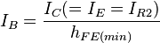
(IR2 is also the emitter current and is assumed to be the same as the collector or required load current, provided hFE is sufficiently large). Resistance R1 at resistor R1 is calculated as

Figure 5: Typical constant current source (CCS) using LED instead of Zener diode
The Zener diode can be replaced by any other diode, e.g. a light-emitting diode LED1 as shown in Figure 5. The LED voltage drop (VD) is now used to derive the constant voltage and also has the additional advantage of tracking (compensating) VBE changes due to temperature. R2 is calculated as

and R1 as
 , where ID is the LED current.

Figure 6: Typical constant current source (CCS) with diode compensation

Figure 7: Typical op-amp current source.
Temperature changes will change the output current delivered by the circuit of Figure 4 because VBE
is sensitive to temperature. Temperature dependence can be compensated
using the circuit of Figure 6 that includes a standard diode D (of the
same semiconductor material as the transistor) in series with the Zener
diode as shown in the image on the left. The diode drop (VD) tracks the VBE changes due to temperature and thus significantly counteracts temperature dependence of the CCS.
Resistance R2 is now calculated as

Since VD = VBE = 0.65 V,[4]

(In practice VD is never exactly equal to VBE and hence it only suppresses the change in VBE rather than nulling it out.)
R1 is calculated as
 (the compensating diode's forward voltage drop VD appears in the equation and is typically 0.65 V for silicon devices.[5])
This method is most effective for Zener diodes rated at 5.6 V or more. For breakdown diodes of less than 5.6 V, the compensating diode is usually not required because the breakdown mechanism is not as temperature dependent as it is in breakdown diodes above this voltage.
Imagine in figure five, at power up, that the LED has 1V across it driving the base of the transistor. At room temperature there is about 0.6V drop across the Vbe junction and hence 0.4V across the emitter resistor, giving an approximate collector (load) current of 0.4/Re amps. Now imagine that the power dissipation in the transistor causes it to heat up. This causes the Vbe drop (which was 0.6V at room temperature) to drop to, say, 0.2V. Now the voltage across the emitter resistor is 0.8V, twice what it was before the warmup. This means that the collector (load) current is now twice the design value! This is an extreme example of course, but serves to illustrate the issue.
The circuit above overcomes the thermal problem. To see how the circuit works, assume Q1 and Q2 are NPN, and voltage has just been applied at V+. Current runs through R to the base of Q1, turning it on and causing current to begin to flow through the load into the collector of Q1. This same load current then flows out of Q1's emitter and consequently through Re to ground. When this current through Re to ground is sufficient to cause a voltage drop that is equal to the Vbe drop of Q2, Q2 begins to turn on. As Q2 turns on it pulls more current through it's collector resistor R, which lowers the voltage at the base of Q1, causing Q1 to conduct less current through the load. This creates a negative feedback loop within the circuit, that keeps the voltage at Q1's emitter almost exactly equal to the Vbe drop of Q2. Since Q2 is dissipating very little power compared to Q1 (since all the load current goes through Q1, not Q2), Q2 will not heat up any significant amount and the reference (current setting) voltage across Re will remain rock steady at ~0.6V, or one diode drop above ground, regardless of the thermal changes in the Vbe drop of Q1. The circuit is still sensitive to changes in the ambient temperature in which the device operates as the BE voltage drop in Q2 varies slightly with temperature.
Conversely, a current source provides a constant current, as long as the load connected to the source terminals has sufficiently low impedance. An ideal current source would provide no energy to a short circuit and approach infinite energy and voltage as the load resistance approaches infinity (an open circuit). An ideal current source has an infinite output impedance in parallel with the source. A real-world current source has a very high, but finite output impedance. In the case of transistor current sources, impedances of a few megohms (at DC) are typical.
An ideal current source cannot be connected to an ideal open circuit because this would create the paradox of running a constant, non-zero current (from the current source) through an element with a defined zero current (the open circuit). Also, a current source should not be connected to another current source if their currents differ but this arrangement is frequently used (e.g., in amplifying stages with dynamic load, CMOS circuits, etc.)
Similarly, an ideal voltage source cannot be connected to an ideal short circuit (R=0), since this would result a similar paradox of finite non zero voltage across an element with defined zero voltage (the short circuit). Also, a voltage source should not be connected to another voltage source if their voltages differ but again this arrangement is frequently used (e.g., in common base and differential amplifying stages).
Contrary, current and voltage sources can be connected to each other without any problems and this technique is widely used in circuitry (e.g., in cascode circuits, differential amplifier stages with common emitter current source, etc.)
Because no ideal sources of either variety exist (all real-world examples have finite and non-zero source impedance), any current source can be considered as a voltage source with the same source impedance and vice versa. These concepts are dealt with by Norton's and Thévenin's theorems.
shows a schematic for an ideal current source driving a
resistor load.
Background
 |
 |
| Voltage source | Current Source |
 |
 |
| Controlled Voltage Source | Controlled Current Source |
| Battery of cells | Single cell |
Figure 2: Source symbols
The internal resistance of an ideal current source is infinite. An independent current source with zero current is identical to an ideal open circuit. The voltage across an ideal current source is completely determined by the circuit it is connected to. When connected to a short circuit, there is zero voltage and thus zero power delivered. When connected to a load resistance, the voltage across the source approaches infinity as the load resistance approaches infinity (an open circuit). Thus, an ideal current source, if such a thing existed in reality, could supply unlimited power and so would represent an unlimited source of energy.
No real current source is ideal (no unlimited energy sources exist) and all have a finite internal resistance (none can supply unlimited voltage). However, the internal resistance of a physical current source is effectively modeled in circuit analysis by combining a non-zero resistance in parallel with an ideal current source (the Norton equivalent circuit). The connection of an ideal open circuit to an ideal non-zero current source does not represent any physically realizable system.
Implementations
Passive current source
The simplest non-ideal current source consists of a voltage source in series with a resistor. The amount of current available from such a source is given by the ratio of the voltage across the voltage source to the resistance of the resistor. This value of current will only be delivered to a load with zero voltage drop across its terminals (a short circuit, an uncharged capacitor, a charged inductor, a virtual ground circuit, etc.) The current delivered to a load with nonzero voltage (drop) across its terminals (a linear or nonlinear resistor with a finite resistance, a charged capacitor, an uncharged inductor, a voltage source, etc.) will always be different. It is given by the ratio of the voltage drop across the resistor (the difference between the exciting voltage and the voltage across the load) to its resistance. For a nearly ideal current source, the value of the resistor should be very large but this implies that, for a specified current, the voltage source must be very large (in the limit as the resistance and the voltage go to infinity, the current source will become ideal and the current will not depend at all on the voltage across the load). Thus, efficiency is low (due to power loss in the resistor) and it is usually impractical to construct a 'good' current source this way. Nonetheless, it is often the case that such a circuit will provide adequate performance when the specified current and load resistance are small. For example, a 5 V voltage source in series with a 4.7 kilohm resistor will provide an approximately constant current of 1 mA (±5%) to a load resistance in the range of 50 to 450 ohm.A Van de Graaff generator is an example of such a high voltage current source. It behaves as an almost constant current source because of its very high output voltage coupled with its very high output resistance and so it supplies the same few microamperes at any output voltage up to hundreds of thousands of volts (or even tens of megavolts) for large laboratory versions.
Active current sources without negative feedback...
In these circuits, the output current is not monitored and controlled by means of negative feedback.Current-stable nonlinear implementation
They are implemented by active electronic components (transistors) having current-stable nonlinear output characteristic when driven by steady input quantity (current or voltage). These circuits behave as dynamic resistors changing its present resistance to compensate current variations. For example, if the load increases its resistance, the transistor decreases its present output resistance (and v.v.) to keep up a constant total resistance in the circuit.Active current sources have many important applications in electronic circuits. They are often used in place of ohmic resistors in analog integrated circuits (e.g., a differential amplifier) to generate a current that depends slightly on the voltage across the load.
The common emitter configuration driven by a constant input current or voltage and common source (common cathode) driven by a constant voltage naturally behave as current sources (or sinks) because the output impedance of these devices is naturally high. The output part of the simple current mirror is an example of such a current source widely used in integrated circuits. The common base, common gate and common grid configurations can serve as constant current sources as well.
A JFET can be made to act as a current source by tying its gate to its source. The current then flowing is the IDSS of the FET. These can be purchased with this connection already made and in this case the devices are called current regulator diodes or constant current diodes or current limiting diodes (CLD). An enhancement mode N channel MOSFET can be used in the circuits listed below.
Following voltage implementation
An example: Bootstrapped current source (Widlar bilateral current source).Voltage compensation implementation

The floating load is a serious disadvantage of this circuit solution.
Current compensation implementation
A typical example are Howland current source[1] and its derivative Deboo integrator.[2] In the last example (see Fig. 1 there), the Howland current source consists of an input voltage source VIN, a positive resistor R, a load (the capacitor C acting as impedance Z) and a negative impedance converter INIC (R1 = R2 = R3 = R and the op-amp). The input voltage source and the resistor R constitute an imperfect current source passing current IR through the load (see Fig. 3 in the source). The INIC acts as a second current source passing "helping" current I-R through the load. As a result, the total current flowing through the load is constant and the circuit impedance seen by the input source is increased.The grounded load is an advantage of this circuit solution.
Current sources with negative feedback
They are implemented as a voltage follower with series negative feedback driven by a constant input voltage source (i.e., a negative feedback voltage stabilizer). The voltage follower is loaded by a constant (current sensing) resistor acting as a simple current-to-voltage converter connected in the feedback loop. The external load of this current source is connected somewhere in the path of the current supplying the current sensing resistor but out of the feedback loop.The voltage follower adjusts its output current IOUT flowing through the load so that to make the voltage drop VR = IOUT.R across the current sensing resistor R equal to the constant input voltage VIN. Thus the voltage stabilizer keeps up a constant voltage drop across a constant resistor; so, a constant current IOUT = VR/R = VIN/R flows through the resistor and respectively through the load.
If the input voltage varies, this arrangement will act as a voltage-to-current converter (voltage-controlled current source VCCS); it can be thought as a reversed (by means of negative feedback) current-to-voltage converter. The resistance R determines the transfer ratio (transconductance).
Current sources implemented as circuits with series negative feedback have the disadvantage that the voltage drop across the current sensing resistor decreases the maximal voltage across the load (the compliance voltage).
Simple transistor current sources
Constant current diode

Due to the large variability in saturation current of JFETs, it is common to also include a source resistor (shown in the image to the right) which allows the current to be tuned down to a desired value.
Zener diode current source

A Zener diode, when reverse biased (as shown in the circuit) has a constant voltage drop across it irrespective of the current flowing through it. Thus, as long as the Zener current (IZ) is above a certain level (called holding current), the voltage across the Zener diode (VZ) will be constant. Resistor R1 supplies the Zener current and the base current (IB) of NPN transistor (Q1). The constant Zener voltage is applied across the base of Q1 and emitter resistor R2.
Voltage across R2 (VR2) is given by VZ - VBE, where VBE is the base-emitter drop of Q1. The emitter current of Q1 which is also the current through R2 is given by


 ,
,
(IR2 is also the emitter current and is assumed to be the same as the collector or required load current, provided hFE is sufficiently large). Resistance R1 at resistor R1 is calculated as

LED current source

and R1 as
, where ID is the LED current.Transistor current source with diode compensation

Resistance R2 is now calculated as
Since VD = VBE = 0.65 V,[4]
(In practice VD is never exactly equal to VBE and hence it only suppresses the change in VBE rather than nulling it out.)
R1 is calculated as
(the compensating diode's forward voltage drop VD appears in the equation and is typically 0.65 V for silicon devices.[5])This method is most effective for Zener diodes rated at 5.6 V or more. For breakdown diodes of less than 5.6 V, the compensating diode is usually not required because the breakdown mechanism is not as temperature dependent as it is in breakdown diodes above this voltage.
Current mirror with emitter degeneration
Series negative feedback is also used in the two-transistor current mirror with emitter degeneration. Negative feedback is a basic feature in some current mirrors using multiple transistors, such as the Widlar current source and the Wilson current source.Constant current source with thermal compensation
One limitation with the circuits in figures five and six is that the thermal compensation is imperfect. In bipolar transistors, as the junction temperature increases the Vbe drop (voltage drop from base to emitter) decreases. In the two previous circuits, a decrease in Vbe will cause an increase in voltage across the emitter resistor, which in turn will cause an increase in collector current drawn through the load. The end result is that the amount of 'constant' current supplied is at least somewhat dependent on temperature. This effect is mitigated to a large extent, but not completely, by corresponding voltage drops for the diode D1 in figure 6, and the LED, LED1 in figure 5. If the power dissipation in the active device of the CCS is not small and/or insufficient emitter degeneration is used, this can become a non-trivial issue.Imagine in figure five, at power up, that the LED has 1V across it driving the base of the transistor. At room temperature there is about 0.6V drop across the Vbe junction and hence 0.4V across the emitter resistor, giving an approximate collector (load) current of 0.4/Re amps. Now imagine that the power dissipation in the transistor causes it to heat up. This causes the Vbe drop (which was 0.6V at room temperature) to drop to, say, 0.2V. Now the voltage across the emitter resistor is 0.8V, twice what it was before the warmup. This means that the collector (load) current is now twice the design value! This is an extreme example of course, but serves to illustrate the issue.
   ----------- V+
   |       |
   R      LOAD
   |       |
   |       C
   --------B Q1
   |       E
   C       |
Q2 B--------
   E       |
   |       Re
   |       |
   ----------- GND
File:Thermalcurrentsource.png
The circuit above overcomes the thermal problem. To see how the circuit works, assume Q1 and Q2 are NPN, and voltage has just been applied at V+. Current runs through R to the base of Q1, turning it on and causing current to begin to flow through the load into the collector of Q1. This same load current then flows out of Q1's emitter and consequently through Re to ground. When this current through Re to ground is sufficient to cause a voltage drop that is equal to the Vbe drop of Q2, Q2 begins to turn on. As Q2 turns on it pulls more current through it's collector resistor R, which lowers the voltage at the base of Q1, causing Q1 to conduct less current through the load. This creates a negative feedback loop within the circuit, that keeps the voltage at Q1's emitter almost exactly equal to the Vbe drop of Q2. Since Q2 is dissipating very little power compared to Q1 (since all the load current goes through Q1, not Q2), Q2 will not heat up any significant amount and the reference (current setting) voltage across Re will remain rock steady at ~0.6V, or one diode drop above ground, regardless of the thermal changes in the Vbe drop of Q1. The circuit is still sensitive to changes in the ambient temperature in which the device operates as the BE voltage drop in Q2 varies slightly with temperature.
Op-amp current sources
The simple transistor current source from Figure 4 can be improved by inserting the base-emitter junction of the transistor in the feedback loop of an op-amp (Figure 7). Now the op-amp increases its output voltage so that to compensate VBE. The circuit is actually a buffered non-inverting amplifier driven by a constant input voltage. It keeps up this constant voltage across the constant sense resistor. As a result, the current flowing through the load is constant as well; it is exactly the Zener voltage divided by the sense resistor. The load can be connected either in the emitter (Figure 7) or in the collector (Figure 4) but in both the cases it is floating as in all the circuits above. The transistor is not needed if the required current doesn't exceed the sourcing ability of the op-amp. The article on current mirror discusses another example of these so-called gain-boosted current mirrors.
Voltage regulator current sources
The general negative feedback arrangement can be implemented by an IC voltage regulator (LM317 voltage regulator on Figure 8). As the bare emitter follower and the precise op-amp follower above, it keeps up a constant voltage drop (1.25 V) across a constant resistor (1.25 Ω); so, a constant current (1 A) flows through the resistor and the load. The LED is on when the voltage across the load exceeds 1.8 V (the indicator circuit introduces some error). The grounded load is an important advantage of this solution.Current and voltage source comparison
Most sources of electrical energy (mains electricity, a battery, ...) are best modeled as voltage sources. Such sources provide constant voltage, which means that as long as the amount of current drawn from the source is within the source's capabilities, its output voltage stays constant. An ideal voltage source provides no energy when it is loaded by an open circuit (i.e. an infinite impedance), but approaches infinite power and current when the load resistance approaches zero (a short circuit). Such a theoretical device would have a zero ohm output impedance in series with the source. A real-world voltage source has a very low, but non-zero output impedance: often much less than 1 ohm.Conversely, a current source provides a constant current, as long as the load connected to the source terminals has sufficiently low impedance. An ideal current source would provide no energy to a short circuit and approach infinite energy and voltage as the load resistance approaches infinity (an open circuit). An ideal current source has an infinite output impedance in parallel with the source. A real-world current source has a very high, but finite output impedance. In the case of transistor current sources, impedances of a few megohms (at DC) are typical.
An ideal current source cannot be connected to an ideal open circuit because this would create the paradox of running a constant, non-zero current (from the current source) through an element with a defined zero current (the open circuit). Also, a current source should not be connected to another current source if their currents differ but this arrangement is frequently used (e.g., in amplifying stages with dynamic load, CMOS circuits, etc.)
Similarly, an ideal voltage source cannot be connected to an ideal short circuit (R=0), since this would result a similar paradox of finite non zero voltage across an element with defined zero voltage (the short circuit). Also, a voltage source should not be connected to another voltage source if their voltages differ but again this arrangement is frequently used (e.g., in common base and differential amplifying stages).
Contrary, current and voltage sources can be connected to each other without any problems and this technique is widely used in circuitry (e.g., in cascode circuits, differential amplifier stages with common emitter current source, etc.)
Because no ideal sources of either variety exist (all real-world examples have finite and non-zero source impedance), any current source can be considered as a voltage source with the same source impedance and vice versa. These concepts are dealt with by Norton's and Thévenin's theorems.
No comments:
Post a Comment